- 您现在的位置:买卖IC网 > Sheet目录3893 > PIC16F723A-I/SS (Microchip Technology)MCU PIC 7KB FLASH XLP 28-SSOP
PIC16(L)F722A/723A
DS41417B-page 10
2010-2012 Microchip Technology Inc.
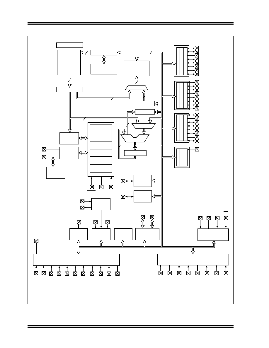
FIGURE 1-1:
PIC16(L)F722A/723A BLOCK DIAGRAM
13
Data Bus
8
14
Program
Bus
Instruction reg
Program Counter
8 Level Stack
(13-bit)
Direct Addr
7
RAM Addr
9
Addr MUX
Indirect
Addr
FSR reg
STATUS reg
MUX
ALU
W reg
Power-up
Timer
Oscillator
Start-up Timer
Power-on
Reset
Watchdog
Timer
Instruction
Decode &
Control
Timing
Generation
OSC1/CLKIN
OSC2/CLKOUT
MCLR VDD
PORTA
RA4
RC0
RC1
RC2
RC3
RC4
RC5
RC6
RC7
8
Brown-out
Reset
AUSART
Timer0
Timer1
Timer2
RA3
RA1
RA0
8
3
Analog-To-Digital Converter
RA6
RA7
RB6
RB7
VSS
T0CKI
T1G
T1CKI
VREF
Synchronous
SDA SCL
SS
SDO
Serial Port
SDI/ SCK/
TX/CK RX/DT
Internal
Oscillator
Block
Configuration
13
Data Bus
8
14
Program
Bus
Instruction reg
Program Counter
8 Level Stack
(13-bit)
Direct Addr
7
RAM Addr
Addr MUX
Indirect
Addr
FSR reg
STATUS reg
MUX
ALU
W reg
Power-up
Timer
Oscillator
Start-up Timer
Power-on
Reset
Watchdog
Timer
Instruction
Decode &
Control
Timing
Generation
MCLR VDD
RC1
8
Brown-out
Reset
AUSART
Timer0
Timer1
Timer2
8
3
VSS
T0CKI
T1CKI
Synchronous
SDA SCL
SS
SDO
Serial Port
SDI/ SCK/
Internal
Oscillator
Block
Configuration
13
Data Bus
8
14
Program
Bus
Instruction Reg
Program Counter
8 Level Stack
(13-bit)
Direct Addr
7
RAM Addr
Addr MUX
Indirect
Addr
FSR Reg
STATUS Reg
MUX
ALU
W Reg
Power-up
Timer
Oscillator
Start-up Timer
Power-on
Reset
Watchdog
Timer
Instruction
Decode and
Control
Timing
Generation
MCLR VDD
PORTB
PORTC
RA5
8
Brown-out
Reset
Timer0
Timer1
Timer2
RA2
8
3
RB0
RB1
RB2
RB3
RB4
RB5
VSS
T0CKI
T1CKI
Synchronous
SDA SCL
SS
SDO
Serial Port
SDI/ SCK/
Internal
Oscillator
Block
Configuration
CCP2
Timer1
32 kHz
Oscillator
PORTE
RE3
CCP1
T1OSI
T1OSO
AN9
AN0 AN1 AN2 AN3 AN4 AN8
AN10 AN11 AN12 AN13
LDO(1)
Regulator
Flash
Program
Memory
Note
1:
PIC16F722A/723A only.
RAM
Capacitive Sensing Module
CPS6
CPS0 CPS1 CPS2 CPS3 CPS4 CPS5
CPS7
发布紧急采购,3分钟左右您将得到回复。
相关PDF资料
PIC12C508A-04/SN
IC MCU OTP 512X12 8SOIC
PIC12C509A-04/SM
IC MCU OTP 1KX12 8-SOIJ
PIC16LF627T-04I/SO
IC MCU FLASH 1KX14 COMP 18SOIC
PIC12C509A-04/P
IC MCU OTP 1KX12 8DIP
PIC18LC452T-I/PT
IC MCU OTP 16KX16 A/D 44TQFP
PIC12LF1822-I/MF
IC MCU 8BIT FLASH 8DFN
PIC12F1822-I/P
IC MCU 8BIT FLASH 8PDIP
PIC12F1822-I/MF
IC MCU 8BIT FLASH 8DFN
相关代理商/技术参数
PIC16F723AT-I/ML
功能描述:8位微控制器 -MCU 7KB Flash 1.8V-5.5V. 16 MHz int Osc RoHS:否 制造商:Silicon Labs 核心:8051 处理器系列:C8051F39x 数据总线宽度:8 bit 最大时钟频率:50 MHz 程序存储器大小:16 KB 数据 RAM 大小:1 KB 片上 ADC:Yes 工作电源电压:1.8 V to 3.6 V 工作温度范围:- 40 C to + 105 C 封装 / 箱体:QFN-20 安装风格:SMD/SMT
PIC16F723AT-I/MV
功能描述:8位微控制器 -MCU 7KB Flash 1.8V-5.5V. 16 MHz int Osc RoHS:否 制造商:Silicon Labs 核心:8051 处理器系列:C8051F39x 数据总线宽度:8 bit 最大时钟频率:50 MHz 程序存储器大小:16 KB 数据 RAM 大小:1 KB 片上 ADC:Yes 工作电源电压:1.8 V to 3.6 V 工作温度范围:- 40 C to + 105 C 封装 / 箱体:QFN-20 安装风格:SMD/SMT
PIC16F723AT-I/SO
功能描述:8位微控制器 -MCU 7KB Flash 1.8V-5.5V. 16 MHz int Osc RoHS:否 制造商:Silicon Labs 核心:8051 处理器系列:C8051F39x 数据总线宽度:8 bit 最大时钟频率:50 MHz 程序存储器大小:16 KB 数据 RAM 大小:1 KB 片上 ADC:Yes 工作电源电压:1.8 V to 3.6 V 工作温度范围:- 40 C to + 105 C 封装 / 箱体:QFN-20 安装风格:SMD/SMT
PIC16F723AT-I/SS
功能描述:8位微控制器 -MCU 7KB Flash 1.8V-5.5V. 16 MHz int Osc RoHS:否 制造商:Silicon Labs 核心:8051 处理器系列:C8051F39x 数据总线宽度:8 bit 最大时钟频率:50 MHz 程序存储器大小:16 KB 数据 RAM 大小:1 KB 片上 ADC:Yes 工作电源电压:1.8 V to 3.6 V 工作温度范围:- 40 C to + 105 C 封装 / 箱体:QFN-20 安装风格:SMD/SMT
PIC16F723-E/ML
功能描述:8位微控制器 -MCU 7 KB Flash 18V-55V 16 MHz Int Osc RoHS:否 制造商:Silicon Labs 核心:8051 处理器系列:C8051F39x 数据总线宽度:8 bit 最大时钟频率:50 MHz 程序存储器大小:16 KB 数据 RAM 大小:1 KB 片上 ADC:Yes 工作电源电压:1.8 V to 3.6 V 工作温度范围:- 40 C to + 105 C 封装 / 箱体:QFN-20 安装风格:SMD/SMT
PIC16F723-E/MV
功能描述:8位微控制器 -MCU 7KB Flash 1.8V-5.5V RoHS:否 制造商:Silicon Labs 核心:8051 处理器系列:C8051F39x 数据总线宽度:8 bit 最大时钟频率:50 MHz 程序存储器大小:16 KB 数据 RAM 大小:1 KB 片上 ADC:Yes 工作电源电压:1.8 V to 3.6 V 工作温度范围:- 40 C to + 105 C 封装 / 箱体:QFN-20 安装风格:SMD/SMT
PIC16F723-E/SO
功能描述:8位微控制器 -MCU 7 KB Flash 18V-55V 16 MHz Int Osc RoHS:否 制造商:Silicon Labs 核心:8051 处理器系列:C8051F39x 数据总线宽度:8 bit 最大时钟频率:50 MHz 程序存储器大小:16 KB 数据 RAM 大小:1 KB 片上 ADC:Yes 工作电源电压:1.8 V to 3.6 V 工作温度范围:- 40 C to + 105 C 封装 / 箱体:QFN-20 安装风格:SMD/SMT
PIC16F723-E/SP
功能描述:8位微控制器 -MCU 7 KB Flash 18V-55V 16 MHz Int Osc RoHS:否 制造商:Silicon Labs 核心:8051 处理器系列:C8051F39x 数据总线宽度:8 bit 最大时钟频率:50 MHz 程序存储器大小:16 KB 数据 RAM 大小:1 KB 片上 ADC:Yes 工作电源电压:1.8 V to 3.6 V 工作温度范围:- 40 C to + 105 C 封装 / 箱体:QFN-20 安装风格:SMD/SMT